sábado, 13 de febrero de 2010

LAST, Sapphire (Al2O3), LiAlO2 ,LiGaO2 Crystal Substrates


LSAT (Lanthanum Strontium Aluminum Tantalum oxide) crystal is a newly developed multi-functional substrate for high Tc super conductive film. It is grown by Czockralski method and good quality by accurate controlling of the temperature distribution and growth rate. LSAT crystal has less structure defect, no domain, no twin structure. It also has low dielectric loss in microwave band.
Sapphire (Al2O3) crystal substrate has a combination of optical and physical properties that make it best choice for a variety of demanding applications.It has good thermal properties, excellent electrical and dielectric properties. We supply high quality and low cost Sapphire crystal substrate  
The lattice parameter of Lithium Dioxogallate (LiGaO2) and Lithium Aluminium Oxide (LiAlO2) crystal can match with the Gallium Nitride film very well. The mismatch coefficients are 0.2% and 1.4% only for LiGaO2 and LiAlO2, much smaller than that of the common used substrates such as <0001> sapphire (14%), <100> MgO (3%), <0001> SiC (3.5%). The Gallium Nitride film is a very important material for blue, violet, UV and white LED. A substrate material that matches the film to be grown well is very important to get a nice GaN epitaxial film.


Crystal Properties:
Substrates LAST Sapphire (Al2O3)
Crystal structure Cubic Hexagonal
Melting point 2113 K 2040 oC
Density (g/cm3) 6.74  3.98
Specific heat 0.57 J/g.k (@ 295 K)
Thermal conductivity 5.1 W/m.k  25.12 (@100 oC)
Thermal Exp.coe.(10-6 /k) 8.2  (@ 295 K) 5.8
Cell parameter (Å) a=b=5.468, c=7.729 a=4.748, c=12.97
Hardness (Mohs) 6.5 9
Orientation <100>,<110>,<111>
Substrates LiAlO2 LiGaO2
Crystal structure mm2 orthorhomnic 422 tetragonal
Melting point 1900 oC 1600 oC
Density (g/cm3) 4.187 2.615
Specific heat 11.8 (@300 K) 7.1 (@393~973 K)
Cell parameter (Å a = 5.1687 Å a = 5.402 Å
Hardness (Mohs) 5 6.5
Orientation <100>,<110>,<111> <100>,<110>,<111>
Last crystals typical sizes (mm): 15x15, 10x10, 10x5, 10x3 
Sapphire (Al2O3) typical sizes (mm): 10x3, 10x5, 10x10, 15x15, 20x15, 20x20, ø15, ø20, ø1", ø2" 
LiAlO2, LiGaO2 typical sizes (mm): 10x3,10x5,10x10,15x15, ø10, ø15
Thickness (mm): 0.5, 1.0 
Fuente: http://www.toplent.com/last.htm
Nombre: Franklin J. Quintero
Asignatura: EES


Connect to the next generation of MSN Messenger  Get it now!

A GaInN/GaN/AlGaN photodetector structure

Structure of the layers.


Scheme of the structure


TEM image of the QW (made by J. Borysiuk)
The sample has been grown by Metal-Organic Chemical Vapour Deposition by P. Caban in Institute of Electronic Materials Technology (ITME), Warsaw, Poland


Interferences in the buffer layer.

The sample is very flat. So it is possible to observe nice interferences. Light is reflected from upper surface of the sample and from GaN/sapphire interface. The two beams are very well parallel so they interfere. From the interference pattern, we can determine width of the GaN layer (2.66 μm at the center).


Photograph of interferences made in white light.


Interferences in 532-nm, green light.


Absorption spectra of the sample.


Photoluminescence maps.

Measurements of photoluminescence give information about quality of GaN and GaInN layers. GaN-related peak is at 360 nm. Its intensity and wavelength are nearly constant on whole surface of the sample.


Photoluminescence spectrum. GaN-related peak is at 360 nm. Emission from GaInN QW is at 400 nm.


Map of intensity of the GaN peak.


Map of wavelength of the GaN peak.


GaInN QW related peaks have wavelengths between 390 and 420 nm depending on a position on the sample. the wavelength of emission from QW depends upon width of the well. The broader well - the longer wavelength. The circular shapes on the maps are due to substrate rotation during growth of the sample.


(A) Photograph of the sample. (B) Map of intensity of the GaInN QW peak. (C) Map of wavelength of the GaInN QW peak.

Photoluminescence has been measured by A. Kos and K. P. Korona in Institute of Experimental Physics, Warsaw University, Warsaw, Poland


Fuente: http://info.fuw.edu.pl/~kkorona/det_AlGaInN.html
Nombre: Franklin J. Quintero
Asignatura: EES


Explore the seven wonders of the world Learn more!

Hot STM Studies of MBE growth of Si on Si(001)

We studied the initial stages of Si MBE growth on Si(001) surfaces. In the initial stages of MBE growth at 530 K, many small one-dimensional (1D) islands are formed. The explanation of this curious shape anisotropy has been controversial. On the Si(001)-(2 × 1) surface, the mobility of Si monomers and dimers is high along the dimer rows and low across them. It has been observed that for certain growth conditions, deposited Si atoms form islands a single dimer row wide (1D islands). The long axes of these 1D islands are aligned perpendicular to the substrate dimer rows. It is puzzling that the islands grow perpendicular to the direction of fast diffusion. Because the mobility is high along the rows, one might expect that islands would capture atoms from a greater distance in this direction. This would lead to growth predominantly along the rows, contrary to what is observed.

Mo et al. proposed a kinetic model based on sticking anisotropy to explain the island shape anisotropy. If island ends are stickier than island sides, arriving adatoms stick preferentially to the ends, resulting in the growth of many 1D islands. Tsao and co-workers suggested that an opening or weakening of dimer bonds might explain this sticking anisotropy. Metiu et al. proposed an alternative model based on an exchange mechanism. Metiu suggested that an adatom arriving on the side of a Si island may displace an existing island atom to the top of the island. The displaced atom diffuses rapidly along the top of the island (the direction of fast diffusion) until reaching an end, where it can fall over the edge and stick. Adatoms arriving on island sides are transported to the ends via this exchange mechanism, resulting in enhanced 1D growth. Our ability to track individual islands microscopically with the STM allowed us to test these models directly.


FIG 1. 400 × 400 Å STM Image of the Si(001) surface at 536 K showing many small Si islands. The direction of fast monomer diffusion is parallel to the dimer rows, indicated by the black arrows.
In Fig. 1 we show an image of the Si(001) surface decorated with many Si islands. Islands have grown on the upper and lower terraces with their long axes aligned perpendicular to the substrate dimer rows. According to the simple sticking anisotropy model of 1D island growth, a long 1D island should be no more likely to capture material at its ends than a short one, for both islands have just two ends. The Metiu model, however, implies that the effective end capture probability should increase linearly with length. Because the exchange mechanism transports adatoms arriving on island sides to island ends, doubling an island's length should double the rate at which material is added to its ends. A portion of one movie is shown in Fig. 2. From detailed analysis of many movie images, we found that growth is independent of length, supporting the anisotropic sticking model. One advantage of our method is that we can select and follow just the 1D islands. The simple anisotropic sticking model is therefore confirmed as the cause the island shape anisotropy observed during growth. We then use our data to measure the anisotropic sticking ratio, yielding a sticking anisotropy ratio of 0.019 ± 0.003. Thus, an end site is roughly 50 times more likely to gain a block than a side site.

Figure 2. 800 × 800 Å STM images from a longer movie showing the growth of 1D islands at 523 K. Time advances from left to right. Coverage increases from 0 to 0.07 ML. The movie begins with the clean substrate before deposition. One can follow individual islands from frame to frame as they grow. View Java Applet Movie or View GIF Animation

Figure 3. 800 × 800 Å STM images showing the growth of islands at 533 K. Time advances from left to right. Coverage increases from 0 to 0.1 ML at a rate of approximately 0.01 monolayers deposited per frame. The movie begins with the clean substrate before deposition. At this temperature 1-D islands form and coalesce. View Java Applet Movie or View Gif Animation
This result gives us insight into MBE growth of Si on Si(001). It is known that in step flow growth, type-B step edges grow faster than type-A edges, eventually causing double height steps to form. Although most material arriving at a step edge is incorporated at existing kink sites, the creation of new kinks (by addition of material to previously flat sections) is the rate-limiting step for the advance of the edge. Because the side of a 1D island is a type-A edge, adding a block there is like adding a block to a flat section of a type-A step edge. The end of a 1D island is a type-B edge; adding a block there is similar to adding a block to a flat section of type-B step edge. Thus the rapid growth of the type-B step edge and the highly anisotropic island shapes are both results of the sticking anisotropy.
Our measured sticking anisotropy, together with our previous measurements of edge fluctuations, also provides a detailed quantitative picture of the coarsening of small islands or features on the Si(001) surface. In this case, the type-B edges of each row fluctuate. The rows on the edge of an island fluctuate fastest, and when the ends cross, the entire row disappears (this process is very clear in Java Applet or Gif Animation movie images of island fluctuations) [Pearson 1995b]. Due to the sticking anisotropy, it is then difficult to nucleate a new row, and the island shrinks. This process will hasten the demise of smaller islands at the expense of larger islands and steps.
The actual microscopic mechanism underlying these step fluctuation and growth processes is not currently known. The current models include monomer, dimer, and dimer vacancy diffusion. The low prefactor that we observed for step fluctuations indicates that a multi-atom or collective process is involved. The activation energy of 0.97 eV that we measure is larger than the 0.67 eV estimated for monomer diffusion, and smaller than the dimer dissociation energy. On the other hand, 0.97 eV is very close to the roughly 1 eV activation energy for dimer diffusion. We suggest that for typical conditions, the monomers pair up into dimers.
Further investigation of epitaxial growth's early stages has therefore involved a detailed study of single and two dimer configurations and dynamics. This has lead to our recent observation of a novel dimer diffusion mechanism that provides for crossing substrate rows thereby extending the possible diffusion pathways into two dimensions. The Stealth, or C-type dimer configuration plays a key role in this mechanism. Surprisingly, the C dimer plays a similar role in the transformation between two four-atom configurations, a transformation which we have observed to lead to epitaxial row formation. Especially at elevated temperatures where process rates are increased, a conventional STM's image rate limits its applicability to surface dynamics studies. For this reason we have implemented a tracking technique which allows us to follow individual features along their diffusive paths. This has yielded dimer diffusion and dissociation activation energies.

Fuente: http://groups.physics.umn.edu/stmlab/growth/growth.html
Nombre: Franklin J. Quintero
Asignatura: EES


Invite your mail contacts to join your friends list with Windows Live Spaces. It's easy! Try it!

Epitaxy

Epitaxy refers to the method of depositing a monocrystalline film on a monocrystalline substrate. The deposited film is denoted as epitaxial film or epitaxial layer. The term epitaxy comes from the Greek roots epi, meaning "above", and taxis, meaning "in ordered manner". It can be translated "to arrange upon".
Epitaxial films may be grown from gaseous or liquid precursors. Because the substrate acts as a seed crystal, the deposited film takes on a lattice structure and orientation identical to those of the substrate. This is different from other thin-film deposition methods which deposit polycrystalline or amorphous films, even on single-crystal substrates. If a film is deposited on a substrate of the same composition, the process is called homoepitaxy; otherwise it is called heteroepitaxy.
Homoepitaxy is a kind of epitaxy performed with only one material. In homoepitaxy, a crystalline film is grown on a substrate or film of the same material. This technology is used to grow a film which is more pure than the substrate and to fabricate layers having different doping levels. In academic literature, homoepitaxy is often abbreviated to "homoepi".
Heteroepitaxy is a kind of epitaxy performed with materials that are different from each other. In heteroepitaxy, a crystalline film grows on a crystalline substrate or film of a different material. This technology is often used to grow crystalline films of materials for which single crystals cannot otherwise be obtained and to fabricate integrated crystalline layers of different materials. Examples include gallium nitride (GaN) on sapphire or aluminium gallium indium phosphide (AlGaInP) on gallium arsenide (GaAs).
Heterotopotaxy is a process similar to heteroepitaxy except for the fact that thin film growth is not limited to two dimensional growth. Here the substrate is similar only in structure to the thin film material.
Epitaxy is used in silicon-based manufacturing processes for BJTs and modern CMOS, but it is particularly important for compound semiconductors such as gallium arsenide. Manufacturing issues include control of the amount and uniformity of the deposition's resistivity and thickness, the cleanliness and purity of the surface and the chamber atmosphere, the prevention of the typically much more highly doped substrate wafer's diffusion of dopant to the new layers, imperfections of the growth process, and protecting the surfaces during the manufacture and handling.
Applications

Epitaxy is used in nanotechnology and in semiconductor fabrication. Indeed, epitaxy is the only affordable method of high crystalline quality growth for many semiconductor materials, including technologically important materials as silicon-germanium, gallium nitride, gallium arsenide, indium phosphide and graphene.
Epitaxy is also used to grow layers of pre-doped silicon on the polished sides of silicon wafers, before they are processed into semiconductor devices. This is typical of power devices, such as those used in pacemakers, vending machine controllers, automobile computers, etc.

Methods
Epitaxial silicon is usually grown using vapor-phase epitaxy (VPE), a modification of chemical vapor deposition. Molecular-beam and liquid-phase epitaxy (MBE and LPE) are also used, mainly for compound semiconductors. Solid-phase epitaxy is used primarily for crystal-damage healing.

 Vapor-phase

Silicon is most commonly deposited from silicon tetrachloride in hydrogen at approximately 1200 °C:

SiCl4(g) + 2H2(g) ↔ Si(s) + 4HCl(g)
This reaction is reversible, and the growth rate depends strongly upon the proportion of the two source gases. Growth rates above 2 micrometres per minute produce polycrystalline silicon, and negative growth rates (etching) may occur if too much hydrogen chloride byproduct is present. (In fact, hydrogen chloride may be added intentionally to etch the wafer.) An additional etching reaction competes with the deposition reaction:

SiCl4(g) + Si(s) ↔ 2SiCl2(g)
Silicon VPE may also use silane, dichlorosilane, and trichlorosilane source gases. For instance, the silane reaction occurs at 650 °C in this way:

SiH4 → Si + 2H2
This reaction does not inadvertently etch the wafer, and takes place at lower temperatures than deposition from silicon tetrachloride. However, it will form a polycrystalline film unless tightly controlled, and it allows oxidizing species that leak into the reactor to contaminate the epitaxial layer with unwanted compounds such as silicon dioxide.
VPE is sometimes classified by the chemistry of the source gases, such as hydride VPE and metalorganic VPE.

 Liquid-phase

Liquid phase epitaxy (LPE) is a method to grow semiconductor crystal layers from the melt on solid substrates. This happens at temperatures well below the melting point of the deposited semiconductor. The semiconductor is dissolved in the melt of another material. At conditions that are close to the equilibrium between dissolution and deposition the deposition of the semiconductor crystal on the substrate is slow and uniform. Typical deposition rates for monocrystalline films range from 0.1 to 1 μm/minute. The equilibrium conditions depend very much on the temperature and on the concentration of the dissolved semiconductor in the melt. The growth of the layer from the liquid phase can be controlled by a forced cooling of the melt. Impurity introduction can be strongly reduced. Doping can be achieved by the addition of dopants.
The method is mainly used for the growth of compound semiconductors. Very thin, uniform and high quality layers can be produced. A typical example for the liquid phase epitaxy method is the growth of ternery and quarternery III-V compounds on gallium arsenide (GaAs) substrates. As a solvent quite often gallium is used in this case. Another frequently used substrate is indium phosphide (InP). However also other substrates like glass or ceramic can be applied for special applications. To facilitate nucleation, and to avoid tension in the grown layer the thermal expansion coefficient of substrate and grown layer should be similar.

 Solid-phase

Solid Phase Epitaxy (SPE) is a transition between the amorphous and crystalline phases of a material. It is usually done by first depositing a film of amorphous material on a crystalline substrate. The substrate is then heated to crystallize the film. The single crystal substrate serves as a template for crystal growth. The annealing step used to recrystallize or heal silicon layers amorphized during ion implantation is also considered one type of Solid Phase Epitaxy. The Impurity segregation and redistribution at the growing crystal-amorphus layer interface during this process is used to incorporate low-solubility dopants in metals and Silicon.

Fuente: http://en.wikipedia.org/wiki/Epitaxy
Nombre: Franklin J. Quintero
Asignatura: EES


Discover the new Windows Vista Learn more!

Metalorganic vapour phase epitaxy

Metalorganic vapour phase epitaxy (MOVPE) is a chemical vapour deposition method of epitaxial growth of materials, especially compound semiconductors from the surface reaction of organic compounds or metalorganics and metal hydrides containing the required chemical elements. For example, indium phosphide could be grown in a reactor on a substrate by introducing Trimethylindium ((CH3)3In) and phosphine (PH3). Alternative names for this process include organometallic vapour phase epitaxy (OMVPE), metalorganic chemical vapour deposition (MOCVD) and organometallic chemical vapour deposition (OMCVD). Formation of the epitaxial layer occurs by final pyrolysis of the constituent chemicals at the substrate surface. In contrast to molecular beam epitaxy (MBE) the growth of crystals is by chemical reaction and not physical deposition. This takes place not in a vacuum, but from the gas phase at moderate pressures (2 to 100 kPa). As such this technique is preferred for the formation of devices incorporating thermodynamically metastable alloys. It has become the dominant process for the manufacture of laser diodes, solar cells, and LEDs.
File:MOCVDprocess.jpg
 Reactor components
A reactor is a chamber made of a material that does not react with the chemicals being used. It must also withstand high temperatures. This chamber is composed by reactor walls, liner, a susceptor, gas injection units, and temperature control units. Usually, the reactor walls are made from stainless steel or quartz. To prevent over heating, cooling water must be flowing through the channels within the reactor walls. Ceramic or special glasses, such as quartz, are often used as the liner in the reactor chamber between the reactor wall and the susceptor. A substrate sits on a susceptor which is at a controlled temperature. The susceptor is made from a material resistant to the metalorganic compounds used; graphite is sometimes used. For growing nitrides and related materials, a special coating on the graphite susceptor is necessary to prevent corrosion by ammonia (NH3) gas


  • Gas inlet and switching system. Gas is introduced via devices known as 'bubblers'. In a bubbler a carrier gas (usually nitrogen or hydrogen) is bubbled through the metalorganic liquid, which picks up some metalorganic vapour and transports it to the reactor. The amount of metalorganic vapour transported depends on the rate of carrier gas flow and the bubbler temperature, and is usually controlled automatically and most accurately by using a Piezocon type vapour control system. Allowance must be made for saturated vapours.
  • Pressure maintenance system
  • Gas Exhaust and cleaning System. Toxic waste products must be converted to liquid or solid wastes for recycling (preferably) or disposal. Ideally processes will be designed to minimize the production of waste products.
  • Fuente: http://en.wikipedia.org/wiki/Metalorganic_vapour_phase_epitaxy
  • Nombre: Franklin J. Quintero
  • Asignatura:EES


Explore the seven wonders of the world Learn more!

Hydride Vapour Phase Epitaxy (HVPE)


Oxford Instruments recently acquired Technologies and Devices Inc (TDI). Based at Silver Spring, Maryland, USA, TDI are a world leading company in the development of Hydride Vapour Phase Epitaxy (HVPE) processes and techniques for the production of novel compound semiconductors such as GaN, AlN, AlGaN, InN, InGaN. These materials are used in a variety of applications, the primary ones being solid state lighting, short wavelength optoelectronics and RF power electronics.
 HVPE Wafer  HVPE Wafer  HVPE Wafer
Nitride-based Templates by TDI
The company produces a wide range of materials on different substrates, including the following:

 Templates  Sizes  Applications
GaN on Sapphire 2" to 4" Blue and White LED applications
AlN on Silicon Carbide 2" to 4" Typically used for RF electronic devices such as HEMT
AlGaN on Sapphire 2" or 3" Optoelectronic devices operating in UV spectral region
InN on Sapphire Research grade available in 2" For work on sensors and high frequency electronic devices
InGaN on Sapphire 2" for Green LED Green LED and green laser Developments
The HVPE Process
In the HVPE process, Group III nitrides (e.g., GaN, AlN) are formed by reacting hot gaseous metal chlorides (e.g., GaCl or AlCl) with ammonia gas (NH3) (Refer to diagram below). The metal chlorides are generated by passing hot HCl gas over the hot Group III metals. All reactions are done in a temperature controlled quartz furnace.

e.g., Hot HCl (g) + Ga (l) ------> GaCl (g)
GaCl (g) + NH3 (g) -------> GaN (s) + HCl (g) + H2 (g)

The GaN or AlN templates have been grown on substrates such as SiC or sapphire. p-type GaN or AlN can be achieved by using Mg during the process and n-type by silane gas with Argon as the carrier gas.
Advantages of HVPE
Developed in the 1960s, it was the first epitaxial method used for the fabrication of single GaN crystals. One of the key features of the technique is its high growth rate (at up to 100 µm per hour) which is almost two orders of magnitude faster than typical MOCVD and MBE processes.

The technique is able to produce crack-free, high quality GaN epitaxial layers (e.g., a typical dislocation density can be as low as 107/cm3 for a 10 µm thick GaN template on sapphire.) Figure 1 shows the X-ray diffraction of a 10 µm thick GaN template on sapphire. The narrow FWHM of 250 arcsec measured at w-scan (0002) peak demonstrates excellent material quality.
Another advantage of HVPE is its ability to grow thick, high quality of AlGaN and AlN for use in optoelectronic and RF electronic devices. The technique has been demonstrated by TDI to grow thicker high quality AlGaN-based active regions of shorter wavelength emitters, which have a high radiative recombination efficiency – an essential feature for high-efficiency UV LEDs. Unlike MOCVD, the HVPE process does not involve metalorganics, thus providing a 'carbon-free' environment for epitaxial growth. In addition, the use of gaseous hydrogen chloride also provides an impurity 'self-cleaning' effect, which results in epitaxial layers with low background impurities and more efficient doping level.
TDI has demonstrated the industry's first HVPE-grown, multilayer, submicron AlGaN/GaN heterostructures.

Fuente: http://www.oxford-instruments.com/products/etching-deposition-growth/processes-techniques/hvpe/Pages/hydride-vapour-phase-epitaxy.aspx
Nombre: Franklin J. Quintero
Asignatura: EES


Connect to the next generation of MSN Messenger  Get it now!

Repeated temperature modulation epitaxy for p-type doping and light-emitting diode based on ZnO


Since the successful demonstration of a blue light-emitting
diode (LED)1, potential materials for making short-wavelength
LEDs and diode lasers have been attracting increasing interest
as the demands for display, illumination and information storage
grow2–4. Zinc oxide has substantial advantages including large
exciton binding energy, as demonstrated by effi cient excitonic lasing
on optical excitation5,6. Several groups have postulated the use of
p-type ZnO doped with nitrogen, arsenic or phosphorus7–10, and
even p–n junctions11–13. However, the choice of dopant and growth
technique remains controversial and the reliability of p-type ZnO is
still under debate14. If ZnO is ever to produce long-lasting and robust
devices, the quality of epitaxial layers has to be improved as has been
the protocol in other compound semiconductors15. Here we report
high-quality undoped fi lms with electron mobility exceeding that
in the bulk. We have used a new technique to fabricate p-type ZnO
reproducibly. Violet electroluminescence from homostructural
p–i–n junctions is demonstrated at room-temperature.
Extending semiconductor devices to new compounds
has produced great benefi ts to human life, as exemplifi ed by
modern optoelectronic and high-speed electronic devices for
communications attained by GaAs-based III–V compounds16,
and blue LEDs and lasers realized by GaN (ref. 1). Even widerbandgap
compounds such as diamond, AlxGa1–xN, BN (refs 2–4)
and ZnO have attracted considerable interest for applications in
ultraviolet LEDs and lasers and electronic devices durable at highpower
and/or high-temperature operation. Among them, ZnO has
the following advantages for LEDs and lasers. First, the exciton
binding energy in ZnO is as large as 60 meV and can be increased
to over 100 meV in superlattices17. This exciton stability provides
opportunities for making highly effi cient lasers operable at roomtemperature5,6.
Second, it is possible to tune the bandgap from
3 eV to 4.5 eV in MgxZn1–xO and Zn1–xCdxO alloy fi lms with quite
small lattice mismatch between the two different compositions18–20.
This advantage makes it possible to realize strain-free and highquality
quantum wells. Third, large and high-quality single-crystal
wafers are commercially available.
To harvest these advantages in real devices, a reliable technique
for fabricating p-type doping needs to be established. Compared with
other II–VI semiconductors and GaN, it has been diffi cult to dope
ZnO to produce a p-type semiconductor because of a strong selfcompensation
effect arising from the presence of native defects or
hydrogen impurities21,22. The fi rst p-type ZnO was claimed in fi lms
made by vapour-phase transport7 in NH3, followed by molecularbeam
epitaxy (MBE) using an atomic nitrogen source9. These fi lms
had a hole concentration of 1016–1017 cm–3. There are other claims8,10
that As or P doping can achieve hole concentrations higher than
1 × 1018 cm–3. In the former case, it can be naturally understood that
nitrogen replaces oxygen to generate holes because of similar ionic
radius. But the latter cases have raised the following questions14.
The ionic radii of P and As seem to be too large to occupy the oxygen
site within the wurtzite host lattice and thus to serve as acceptors.
Also, from a comparison with established properties of p-type GaN
(ref. 12), such a high concentration of holes would not be expected
in ZnO. None of the studies mentioned addressed signifi cant effort
to growing the high-quality undoped fi lms that generally serve as
a starting point for reliable doping in semiconductors. Here we
propose a repeated temperature modulation (RTM) technique as a
reliable and reproducible way to fabricate p-type ZnO.
Thin fi lms of ZnO and junction devices were grown by laser
MBE using nitrogen as a p-type dopant (see Methods). Figure 1a
shows a typical intensity oscillation of refl ection high-energy
electron diffraction (RHEED) observed during undoped ZnO fi lm
growth at a temperature (Tg) of 950 °C. This layer-by-layer growth
mode has become possible with our development of an atomically
smooth ZnO buffer layer on ScAlMgO4 (SCAM) substrate produced
by high-temperature annealing23,24. The undoped ZnO fi lms
show excellent optical and electronic properties. Figure 1b shows
a photoluminescence spectrum (inset) and temporal variation
of the photoluminescence intensity taken at room-temperature.
The lifetime (τPL) of free-exciton emission reaches 2.5 ns. This τPL is
much longer than the value in ZnO crystal (1 ns)25 or high-quality
GaN single crystal (0.86 ns)26. Such a long lifetime indicates very
low density of non-radiative defects and negligible carrier trapping
to deep radiative defects, such as the green luminescence band
frequently seen in poor-crystallinity crystals and fi lms. Figure 1c
shows the temperature dependence of residual electron density
(n) and Hall mobility (μ) for an undoped ZnO fi lm. The value of
n is about 1 × 1016 cm–3 at room temperature and decreases with
decreasing temperature, with an activation energy of about 60 meV.
The value of μ is 300 cm2 V–1 s–1 and 5,000 cm2 V–1 s–1 at 300 K and
100 K, respectively, surpassing the best value for a ZnO bulk single
crystal27. Therefore, we conclude that ZnO fi lms grown at this high
temperature, Tg, on atomically smooth buffer layers can serve as an
arena for testing acceptor doping.
However, nitrogen, as one of the most promising acceptor
impurities, cannot be incorporated into ZnO at such a high Tg.
Nitrogen concentration (CN) decreases from a few times 1020 cm–3 at
Tg = 450 °C to a few times 1018 cm–3 at Tg = 700 °C, and at Tg = 950 °C
it is lower than the detection limit (mid-1017 cm–3)28. To solve this
dilemma, we have developed RTM to satisfy both high crystallinity
and high CN. We repeated a growth sequence in which a nitrogendoped
ZnO (ZnO:N) layer 10–15 nm thick is deposited at low
temperature (TL), followed by rapid ramp to high temperature (TH),
and growth of a 1-nm-thick layer at TH. Figure 2a shows an example
of the time variations of RTM. During the processes, the RHEED
pattern switched between two states as shown in the insets of Fig. 2b:
streaks (left) at TL and spots (right) at TH. The streak length, defi ned
by the full width at half maximum of streak intensity peak in the
vertical direction (shown on the insets), is plotted as a function of
time in Fig. 2b. During deposition at TL, the surface became gradually
rougher because of the low surface diffusivity of precursors.
On rapid ramping to TH, the surface smoothness recovered quickly.
Part of the time variation in Fig. 2b is magnifi ed in Fig. 2c (red)
together with the RHEED intensity oscillation (black). The two
oscillation patterns have opposite phase, indicating that initial TL
layers grown on atomically fl at TH layers grew in layer-by-layer mode
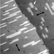
even at such a low temperature. Figure 2d shows an atomic force
microscopy image for a ZnO:N fi lm. The surface is composed of
atomically fl at, wide terraces and 0.26-nm-high islands. By using RTM, we
can grow ZnO:N fi lms with CN ranging from several times 1020 cm–3
to a few times 1018 cm–3 by tuning TL from 400 °C to 600 °C.
Among these fi lms, those grown at TL = 400 °C and TH = 950 °C
reproducibly showed p-type conduction. It is worth mentioning that
TH was chosen to satisfy the condition that hydrogen is completely
extracted from the fi lm29. Because residual hydrogen in the growth
chamber is incorporated in the fi lms during growth21, hightemperature
annealing may be essential not only for annihilating
non-equilibrium defects but also for removing hydrogen, if any, to
activate the acceptors.
The ZnO:N fi lms prepared by RTM have the same in-plane lattice
constant as that of the buffer layer. The out-of-plane lattice constant
is slightly expanded (+0.02%) compared with the bulk value.
The rocking curve width is as narrow as that of the undoped ZnO
fi lms, indicating that the structural quality of the p-type ZnO is very
high. The inset of Fig. 3 shows a set of raw data for the Hall resistance,
indicating p-type conduction as evidenced by the positive slope.
Figure 3 shows hole concentration as a function of temperature for
a p-type ZnO:N fi lm with CN = 2 × 1020 cm–3. From these data, we
can deduce an activation energy EA of 100 meV and compensation
ratio ND/NA ≈ 0.8. Here we note that ND/NA obtained in the present
p-type ZnO fi lm is higher than the reported value of 0.1 for p-type
ZnO grown by MBE9. Therefore, there is still room to increase hole
concentration by tuning the RTM growth condition.
The schematic structure of a typical homostructural p–i–n
junction is shown in Fig. 4a, which was grown throughout in layerby-
layer mode keeping an atomically fl at interface. Figure 4b shows
typical current–voltage characteristics. Fairly good rectifi cation
was obtained with a threshold voltage of about 7 V. The threshold
voltage is higher than the bandgap of ZnO (3.3 eV), mainly owing to
the high resistivity of the p-type ZnO layer. The electroluminescence
is measured by feeding in a direct current at room temperature.
This spectrum was measured from the top by detecting the light
escaping from the edge of the top electrode. The electroluminescence
spectrum shows luminescence from violet to green regions with
multi-refl ection interference fringes. We would expect exciton
emission at 3.2 eV from the undoped layer (i-ZnO) as shown in the
inset of Fig. 1b, but the electroluminescence spectrum apparently
shows a redshift. This is partly due to the low hole concentration in
p-type ZnO: electron injection from i-ZnO to p-type ZnO overcomes
hole injection from p-type ZnO to i-ZnO. The photoluminescence
spectrum (black) of a p-type ZnO fi lm is also shown. The higherenergy
side peak around 430 nm in the electroluminescence
spectrum matches well with the photoluminescence spectrum.
Another factor could be that the electroluminescence from active i-
ZnO is partly absorbed in the p-type layer because of a slight redshift
of the absorption edge for this layer. Nevertheless, the signal-tonoise
ratio of the electroluminescence spectrum shown in Fig. 4c is
much better than those reported previously11,30. More importantly,
the RTM technique established for reliable p-type doping of ZnO
enables us to improve the device performance further by optimizing
the growth parameters and device structures.
The next challenge will be to increase the hole concentration
by further optimizing the growth process of p-type ZnO.
Making a p-type (Mg,Zn)O fi lm is also an important challenge, not
only to prevent the majority of electrons from injecting into the
p-type layers, but also to avoid attenuation of band-edge emission
from the i-ZnO.

Figure 1 Thin fi lms of ZnO grown in persisting layer-by-layer mode show
high-quality optical and electronic properties. a, RHEED intensity oscillation
observed during ZnO thin-fi lm growth by laser MBE at a temperature of 950 °C on an
atomically smooth ZnO buffer layer formed on a ScAlMgO4 substrate. The oscillation
period corresponds to a 0.26-nm-thick charge-neutral molecular layer grown by
about 23 laser pulses. The oscillation persisted over fi lm growth to a thickness of
1 μm. The fi lm has the same lattice constants (a = 0.3250 nm, c = 0.5204 nm) as
the bulk values by relaxing the very small lattice mismatch of 0.09% with the SCAM
substrate in the high-temperature annealed ZnO buffer layer. The full-width at halfmaximum
of the rocking curve at the (002) refl ection is less than 18 arcsec, which
is close to the instrumental resolution. The growth direction is identifi ed, through
experiments similar to those reported previously32, to be [0001–] of the wurtzite
structure (oxygen face). b, Photoluminescence (PL) spectrum (inset) and temporal
decay of the luminescence intensity at the peak energy (indicated by triangle)
for an intrinsic ZnO fi lm. The dashed peak represents the temporal evolution of
the excitation laser pulse (Ti: sapphire, 242 nm, 30 mW, 80 fs). The lifetime of
free exciton emission exceeds 2.5 ns, indicating the high quality of the sample.
c, Temperature dependence of electron mobility and carrier concentration for an
undoped ZnO fi lm (solid circles) and a ZnO bulk single-crystal (open circles, after
Look et al.27). To ensure that the measurements extract the intrinsic properties of
the ZnO fi lm, a fairly thick fi lm (1 μm) was grown on a semi-insulating Mg0.15Zn0.85O
buffer layer which was annealed to prepare an atomically smooth surface before
the ZnO deposition23.

Figure 2 Atomically smooth ZnO fi lms doped with nitrogen can be grown by
a repeated temperature modulation technique. a, Temporal variation of growth
temperature, switching between TH and TL, during ZnO thin-fi lm growth. Layers
of ZnO:N with high nitrogen concentration (CN) were deposited at TL in the period
coloured blue. The layers were annealed and additional ZnO:N layers with low CN
were grown in the period coloured red in order to activate nitrogen as an acceptor
and recover surface smoothness, respectively. b, Typical RHEED patterns observed
during TL (left) and TH (right) periods are shown in the insets, representing rather
rough and atomically smooth surfaces by streaky and spotty patterns, respectively.
Temporal variation of streak length (defi ned by broken lines) is plotted as a measure
of the surface roughness. c, RHEED intensity (black) and streak length (red) are
plotted for the initial growth of high CN layer at TL as denoted by circle in b. Clear
oscillations having a half-phase shift confi rm the layer-by-layer growth mode.
d, An AFM image of the surface for a 500-nm-thick ZnO:N fi lm. The step height
corresponds to the thickness of a charge-neutral molecular layer of ZnO (0.26 nm).

Figure 3 Temperature dependence of hole concentration (p) in a p-type
ZnO doped with nitrogen. (Nitrogen concentration CN = 2 × 1020 cm–3.) A typical
variation of the Hall voltage during a magnetic fi eld scan is shown in the inset.
The hole mobility varies from 5 cm2 V–1 s–1 at 350 K to 8 cm2 V–1 s–1 at 300 K.
Activation energy EA and compensation ratio ND/NA are deduced to be 100 meV and
0.8, respectively, from the linear fi tting9 of p = (ND/NA – 1)(gA1/gA0)NvT3/2 exp(–EA/kBT),
where gA0 = 4 and gA1 = 1 are the unoccupied and occupied state degeneracies,
respectively, NvT3/2 = 2(2πmhkBT/h2)3/2 is the density of states in the valence band,
where kB is Boltzmann's constant and h denotes Planck's constant, and mh is
assumed to be 0.9m0 with m0 being free electron mass.

Figure 4 Zinc oxide homostructural p–i–n junction shows rectifying
current–voltage characteristics and electroluminescence (EL) in forward
bias at room-temperature. a, The structure of a typical p–i–n junction LED.
b, Current–voltage characteristics of a p–i–n junction. The inset has logarithmic scale
in current with F and R denoting forward and reverse bias conditions, respectively.
c, Electroluminescence spectrum from the p–i–n junction (blue) and
photoluminescence (PL) spectrum of a p-type ZnO fi lm measured at 300 K.
The p–i–n junction was operated by feeding in a direct current of 20 mA.

Nombre: Franklin J. Quintero
Asignatura: EES


Connect to the next generation of MSN Messenger  Get it now!