Most of the rapid developments in (AlIn)GaN alloy system technology have occurred within the past few years, and the technology is still moving at a fast pace. New performance records for light-emitting diodes and laser diodes are constantly being reported. This article highlights the progression of the development of the (AlIn)GaN alloy system and describes the fabrication and performance of some of the light-emitting devices that have been produced to date.
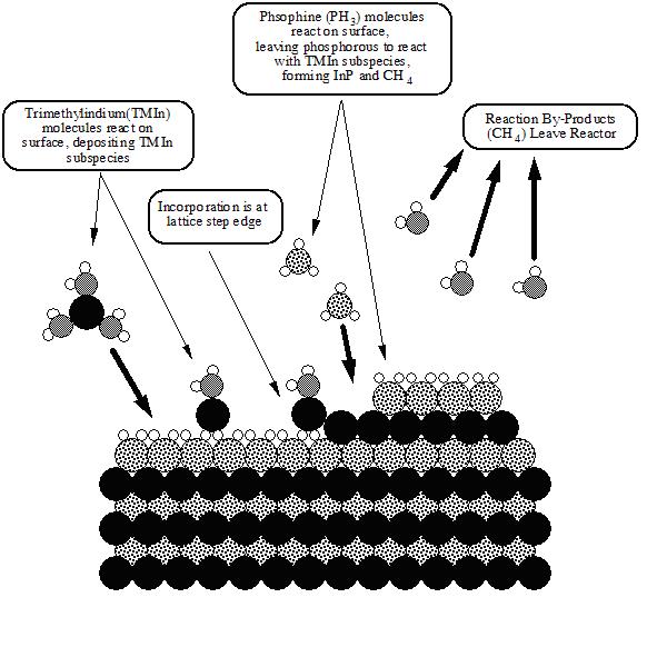
Since the invention of the incandescent electric lamp by Thomas Edison in 1879, there has been a drive for less expensive, more reliable, and brighter lighting sources. Massive industries have been created to produce filament and fluorescent lamps for interior applications, sodium-discharge lamps for streets, and neon signs for ever-popular exterior advertising. The most recent revolutionary lighting advancement is the light-emitting diode (LED). Initially demonstrated in 1962, the LED1 and its companion, the laser diode (LD),2,3 have been used in such diverse applications as optical-fiber communication networks, instrument-panel indicators, CD optical-storage technology, laser printers, and automobile tail lights and brake lights. Originally restricted to the color red, yellow, orange, and amber LEDs with light-emission efficiencies superior to incandescent lamps became commercially available by the early 1990s,4 spawning a market valued at well over $1 billion a year.5 That market is expected to undergo tremendous growth as LEDs continue to infiltrate the full-color outdoor display, traffic signal, and automotive interior and exterior lighting markets. While the technological growth of red and yellow LEDs has been meteoric in the past decade, the push to extend operation into the short wavelength region of the visible spectrum (from green to violet) has proven very challenging. Although successful attempts to make LEDs and LDs with SiC and II-VI materials (e.g., ZnSe) have been made, the utility of such devices has been diminished by the very low efficiency in SiC diodes and the short device lifetimes in the II-VI materials due to the relative ease of defect formation. As a result, the III-V nitride materials with the wurtzite crystal structure (GaN, AlN, InN, and their alloys) have generated considerable interest for operation at these wavelengths. Since the electronic band structure for each of the nitride materials possesses a direct transition with a band gap energy ranging from 1.9 eV for InN, to 3.4 eV for GaN, to 6.2 eV for AlN at room temperature as well as a fairly high thermal conductivity, the (AlIn)GaN system has been explored in the areas of high-power and high-temperature electronic devices and short-wavelength (visible and ultraviolet) optoelectronic devices. (For an excellent review of relevant properties, consult Reference 6.) Considerable efforts to produce and characterize the nitrides began in earnest more than 30 years ago at a number of notable research facilities, such as AT&T Bell Laboratories, IBM Thomas J. Watson Research Center, and RCA, because of the potential for producing surface acoustic wave devices, blue lasers, and LEDs. Most of these programs, however, were eventually canceled due to the inability to solve several key technological problems that hampered development. Since there was no suitable bulk-crystal technology for producing GaN substrates, epitaxy was done on highly lattice- and thermal-expansion-mismatched substrates such as silicon, gallium arsenide, and sapphire. The resulting heteroepitaxial films were invariably highly defected with ~1010 dislocations/cm2 and highly conducting as a result of defects and impurities. The films also exhibited poor surface morphology as a result of a nonoptimized growth approach. The high n-type background, coupled with the relatively deep ionization levels of common p-type impurities, resulted in an inability to grow p-type material and prevented the development of bipolar and injection-type devices. Despite these problems, the fabrication of metal-insulator-semiconductor LEDs was achieved, thus demonstrating the potential for this material system.7 It was not until the mid-1980s that these problems began to be overcome, due in large part to the efforts of Isamu Akasaki at Nagoya and Meijo Universities and a group led by Shuji Nakamura at Nichia Chemical Company. The use of thin, low-temperature AlN8 and, later, GaN9 buffer layers facilitated the growth of high-quality GaN films, specular and free of cracks, on sapphire substrates by metalorganic chemical vapor deposition (MOCVD). Simultaneously, remarkable improvements in the electrical and optical properties were demonstrated. Another monumental breakthrough was the first successful production of p-type GaN by low-energy electron-beam irradiation (LEEBI) of magnesium-doped GaN, which in the as-grown state exhibits high resistivity.10 As a result, the first GaN electroluminescent device based on a p-n junction was demonstrated. Subsequently, it was shown that magnesium-doped GaN could also be made conductive by thermal annealing in a N2 ambient at a temperature of about 600°C.11 These developments, along with the fact that light-generation processes in the nitride material seem unaffected by the high dislocation density commonly found in the epitaxial films, have allowed the demonstration and commercialization of high-brightness blue and green double heterostructure12 and single quantum well (SQW)13 LEDs in the past few years as well as the demonstration of the first violet (~420 nm) room-temperature, continuous-wave (CW) LD in 1996.14 When combined with the red, orange, and yellow LEDs and LDs, these breakthroughs set the stage for another photonic technology revolution. Several techniques have been used for the epitaxial growth of III-V nitride semiconductors. Among these techniques, molecular-beam epitaxy and MOCVD have been the most popular, mainly due to their wide use in the fabrication of most III-V compound semiconductors. However, MOCVD may be more suitable for high-volume production for this material system for two reasons: higher throughput (lower cost) and demonstrated superior material quality.8,15-18 In an MOCVD process, the film is deposited through a chemical reaction occurring between metalorganic precursors and hydrides on a hot substrate surface. In the case of (AlIn)GaN crystal growth, TMGa, TMAl, and TMIn are normally used as group III precursors, while NH3 is used as a nitrogen source. GaN, for example, can be grown by introducing TMGa and NH3 simultaneously into the reaction chamber with a substrate, such as sapphire, heated to elevated temperatures (usually 800-1,000°C). Ternary compounds such as AlGaN and InGaN can be obtained by blending TMAl or TMIn simultaneously with TMGa. The solid composition is controlled by adjusting the gas-phase composition of the TMAl and TMGa or the TMIn and TMGa.
Although the MOCVD epitaxial growth principle is simple, researchers faced several challenges in the 1980s to achieve device-quality nitride thin films. One of the difficulties was that ammonia is a very stable molecule, and its cracking efficiency is low. In order to maintain the solid stoichiometry in the grown film, very high ammonia partial pressure in the growth ambient is required. Usually, a high volume of ammonia and a high growth temperature (enhancing thermal decomposition) are used in the growth process. However, when the growth ambient (usually a mixture of ammonia and hydrogen) consists of a high concentration of ammonia (normally 50%), physical properties of the ammonia will have a dominant effect on the flow dynamics in the reactor. This is not the case for the MOCVD growth of other III-V compounds such as GaAs or InP, where the concentrations of AsH3 and PH3 in the reactor are in the 0.01% range in a hydrogen ambient. Because ammonia has a higher density and a much lower thermal conductivity than hydrogen, the flow is apt to be turbulent (large Reynolds number). The situation becomes even worse at high growth temperatures where thermal convection can cause even more turbulent flow. 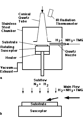
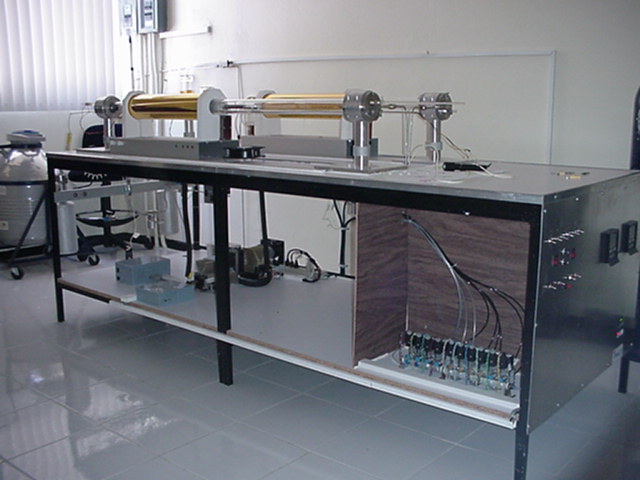
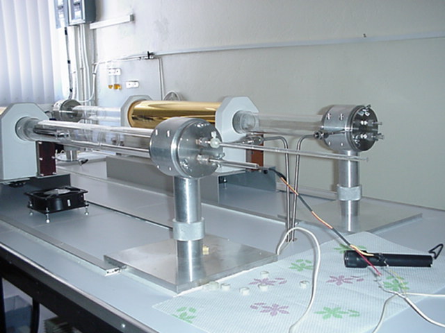
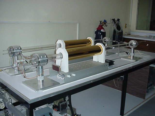
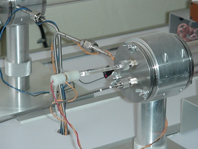
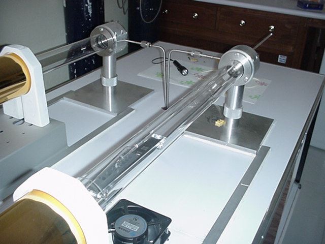
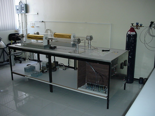
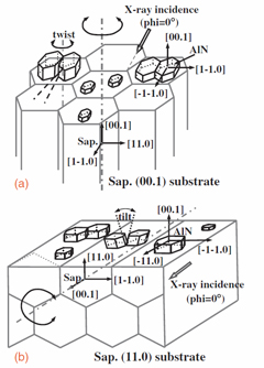
In early 1990, Nakamura et al.16 reported a novel two-flow reactor design that addressed this problem (Figure 1). The source gases (main flow) were introduced parallel to the substrate surface similar to the conventional horizontal reactor. A second flow (subflow) consisting of equal amounts of N2 and H2was introduced from above, perpendicular to the substrate surface, to suppress any thermal convection arising from the heated substrate (1,000°C) and to bring the reactants toward the substrate surface. Without the subflow, the growth was not two-dimensional, and only GaN islands were formed. A second problem for growing III-V nitride films is the lack of a suitable substrate that matches the lattice constant and thermal-expansion coefficient of the GaN films. In the mid-1980s, the Japanese research group led by Akasaki at Meijo University developed a two-step MOCVD process using a c-plane sapphire substrate. They grew a thin (200Å) AlN buffer layer at low temperature followed by a high-temperature thick layer of GaN.8 Mirror-like GaN films with improved optical and electrical properties were obtained. The use of the thin buffer layer was believed to enhance the two-dimensional nucleation so that a layer-by-layer growth mechanism could be achieved. In early 1990, Nakamura and coworkers at Nichia Chemical Company used a similar approach in which a GaN buffer layer was grown at low temperature.9 High-quality n-type GaN films were achieved with background carrier concentrations of 4 x 1016cm-3 and Hall mobilities around 600 cm2/V · s, despite high dislocation densities of 109-1010 cm2 in the films. Heteroepitaxially grown GaN films on sapphire substrates contain high densities of structural line and planar defects. The structural properties of these layers have been extensively studied with transmission electron microscopy.19,20 Most dominant are threading dislocations that are nearly parallel to the c axis. Their density ranges between 108 dislocations/cm2 and 1010 dislocations/cm2 even after several micrometers of film growth.19 Depending on the substrate preparation, stacking faults and edge dislocations are present near the interface with the sapphire substrate.20 Inversion domain boundaries have also been reported for III-V nitrides in the literature.21 These structural defects are generated due to the small lattice constants of III-V nitrides resulting in a large lattice (~14%) and thermal-expansion-coefficient mismatch (~80%) with sapphire.19 In planar-view transmission electron micrographs taken several micrometers away from the GaN/sapphire interface, the threading dislocations tend to appear in cellular arrangements suggesting a columnar or cell-type structure of heteroepitaxial GaN films. 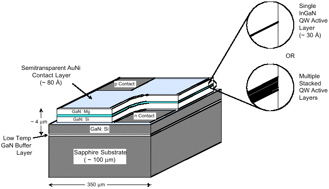
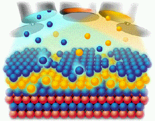
ontrary to other materials used for minority-carrier optoelectronic device applications, such as III-V arsenides or III-V phosphides, where dislocation densities above 104 cm-2 adversely affect the device performance, the realization of bright LEDs with long life is possible with III-V nitrides.13 It has been demonstrated that threading dislocations cross through the InGaN active layer of high-performance blue LEDs, which exhibit external quantum efficiencies as high as ~3% at 20 mA.22 It appears that dislocations in III-V nitrides are not associated with electrically active defects that would act as effective nonradiative recombination centers and effectively limit the lifetime of minority carriers. For blue and green LEDs, InGaN films with high indium content are required. Nakamura and coworkers describe the growth of high-quality InGaN films23 by adjusting the growth rate and growth temperatures to optimize material quality and emission wavelength. With all the building blocks available, high-efficiency commercial blue and green nitride-based LEDs are currently available from more than one source. The brightest devices use either a single or multiple quantum well structure (Figure 2). A typical complete device structure consists of a low-temperature deposited GaN or AlN buffer layer on c-plane sapphire, a 3-4 µm silicon-doped GaN layer, a SQW or multiple quantum well (MQW), a 1,000Å magnesium-doped AlGaN layer, and a 3,000Å magnesium-doped GaN layer.
The formative stage of any semiconductor device technology requires the selection and characterization of dopants. Both impurities and native defects may act as donors or acceptors and affect the electrical conductivity of semiconductors. The species of dopant is chosen to best achieve the desired device performance, and controlled introduction of the dopant is required for reproducible characteristics. Undoped GaN films are usually n-type; contamination with silicon or oxygen, which act as donors, has been identified as the reason for this. Silicon and magnesium, which substitute for gallium in the GaN lattice, are the donor and acceptor of choice for doping III-V nitrides n- and p-type, respectively.24-26 However, all devices grown with techniques that use NH3 as a nitrogen source or that furnish a hydrogen-rich ambient, such as MOCVD, require an additional, deliberate processing step to electrically activate the acceptor dopant. These processes are either LEEBI10 or thermal annealing above 600°C in an N2 ambient.11,27 It has been shown that the formation of electrically inactive acceptor-hydrogen complexes during MOCVD growth is responsible for the observed low p-type doping efficiency in as-grown GaN.28 The LEEBI or heat treatment dissociates acceptor-hydrogen complexes and, thereby, electrically activates the acceptor dopants, as has been observed for other semiconductors (e.g., GaAs:Zn).29 The conventional Hall-effect technique is a well-established, powerful tool to investigate the electrical properties of shallow dopants in semiconductors, especially when performed over a range of temperatures. The analysis of the temperature dependence of the carrier concentration enables the determination of important dopant parameters, such as the concentration and thermal activation energy for dopant ionization, and the concentration of compensating donors or acceptors.30 Properties of silicon donors and magnesium acceptors in GaN have been investigated with variable-temperature Hall-effect measurements conducted in the temperature range of 100-700 K with a magnetic field of 12.5 kG or 17 kG. Combined with secondary ion mass spectrometry (SIMS) analysis, which yields quantitative silicon or magnesium profiles in the epitaxial films when calibrated with implantation standards, detailed properties of the dopants have been determined. 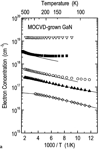
Results from variable-temperature Hall-effect measurements for n-type GaN are shown in Figure 3. Sample one was unintentionally doped, and samples two through five were silicon-doped. The electron concentrations are shown as functions of the reciprocal temperature, and the electron mobilities are shown as functions of temperature. The unintentionally doped GaN film exhibits the lowest electron concentration (~5 x 1016 cm-3, 300 K) and the highest electron mobility (~650 cm2/V s, 300 K). The silicon-doped samples show higher electron concentrations and lower electron mobilities. The silicon doping level was gradually increased from sample two to sample five. Consequently, the electron concentrations increase accordingly as determined by the Hall-effect measurements. Sample five shows an electron concentration of ~2 x 1019 cm-3, which is temperature independent. Such behavior is typically observed for degenerately doped semiconductors.
The peak mobilities for the n-type GaN samples shown in Figure 3 range from 135 cm2/V s (sample five, 300 K) to 1,450 cm2/V s (sample one, 130 K) and decrease with increasing electron concentration. The solid lines in Figure 3a are the result of a least-squares fit of the charge-neutrality condition30 to experimental n(T) data of samples one through four. The fit yields parameters for a shallow donor level that is dominant in the GaN films, and modeling yields activation energies for the shallow level of 16 meV (sample one), 14 meV (sample two), 12 meV (sample three), and 7 meV (sample four). The concentration of the shallow donor level is 6 x 1016 cm-3, 2.3 x 1017 cm-3, 7.4 x 1017 cm-3, and 7.9 x 1018 cm-3 in samples one through four, respectively. The presence of a second donor level had to be assumed to model the temperature dependence of the electron concentrations of samples one through three. The activation energy for this donor level ranges from 32 meV to 37 meV and its concentration ranges from 3 x 1016 cm-3 to 6 x 1016 cm-3, independent of the silicon doping. It is possible that this is due to oxygen substituting for nitrogen in the GaN lattice acting as a donor.
Magnesium-doped GaN samples (samples six through eight) are shown in Figure 4. The p-type conductivity for all three samples was activated by thermal annealing. The hole concentration is shown as a function of reciprocal temperature, and the hole mobility is shown as a function of temperature. Sample six exhibits the highest hole concentration and the lowest hole mobility. At 300 K, the hole concentration is ~8 x 1017 cm-3 and the mobility is only ~3 cm2/V s. The analysis of the temperature dependence of the hole concentration at temperatures above 280 K using the charge-neutrality condition30 is consistent with the presence of a single acceptor with an activation energy of ~160 meV and a concentration of ~8 x 1019 cm-3 (solid line). The elemental magnesium concentration as determined by SIMS was found to be ~1 x 1020 cm-3. For magnesium-doped GaN, good agreement is typically found between the concentration of magnesium and the concentration of the dominant-acceptor level, the latter determined by analysis of the Hall-effect data. This indicates that most of the magnesium atoms are incorporated on gallium lattice sites and act as acceptors. For samples six and seven at temperatures below ~280 K, the temperature dependence of the hole concentration is not accurately described by the ionization of an acceptor due to hopping conduction via closely spaced acceptor states. For sample eight, however, the temperature dependence of the hole concentration can be described over the entire temperature range of the Hall-effect data. The analysis reveals that the acceptor concentration of sample eight is lower than in sample six. For samples seven and eight, the acceptor concentration is ~4 x 1019 cm-3 and ~2 x 1019 cm-3, respectively; the magnesium concentration as measured by SIMS was found to be ~5 x 1019 cm-3 and ~2 x 1019 cm-3, respectively, and the acceptor activation energies were found to be ~170 meV and 175 meV, respectively. 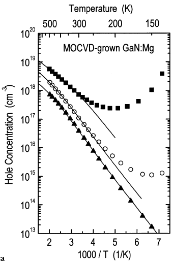
From the analysis of the Hall-effect data, the concentration of compensating donors was found to be greater than 1018 cm-3 for all of the magnesium-doped samples of Figure 4. Possible candidates for compensating donors are the nitrogen vacancy (VN) and substitutional oxygen (ON), the latter exhibiting a strong affinity to magnesium. However, the hole concentration is only marginally affected by the presence of compensation, since the acceptor concentration in magnesium-doped GaN is typically more than one order magnitude higher than that of compensating donors.
The hole mobility is adversely affected by both the presence of compensating donors and high concentrations of acceptors. The 300 K hole mobility for samples seven and eight are ~6 cm2/V s and 15 cm2/V s, respectively. The 300 K resistivity for all three magnesium-doped GaN films depicted in Figure 4 is ~3 W cm. Such a high resistivity constituted one of the main obstacles in achieving low forward voltages in GaN light emitters. The device problem is magnified by the difficulty in forming low-resistance ohmic contacts to magnesium-doped, p-type GaN.
The brightest (AlIn)GaN LEDs are SQW or MQW p-n junctions grown on an electrically insulating sapphire substrate, as shown in Figure 2. Although some manufacturers use conducting SiC as the substrate for the (AlIn)GaN epitaxial growth [the lattice constant of SiC is, in fact, a better match to the (AlIn)GaN epitaxial films than sapphire], up to this point, the best devices have been produced using sapphire as the substrate. In addition, blue (AlIn)GaN solid-state lasers have been demonstrated by several groups.Nichia published the first observation of stimulated emission in a room-temperature (AlIn)GaN MQW violet LD under CW current injection in 1996 (Figure 5).14 Lifetimes of these lasers have recently been reported to exceed 100 hours. In Figures 2 and 5, the electrical contacts to the p- and n-layers are both on the top surface of the device because of the insulating sapphire substrate. Because it is difficult to obtain highly-doped, conducting p-type GaN, the current does not spread laterally within the thin p-layers. Thus, the area of the contact to the p-layer has to be maximized to promote current spreading, which, in turn, maximizes light emission and minimizes turn-on voltage and series resistance. An important consequence for LEDs on sapphire is that since most of the light generated at the junction escapes the device through the top surface, the large-area p-contact has to be made as transparent as possible outside the area where electrical bond wires are attached. Other fabrication challenges include etching (AlIn)GaN (which has a hardness and chemical inertness resembling diamond) to expose the n-layer, etching or cleaving smooth laser facets through the highly-stressed and compositionally diverse active area, thinning the sapphire without breaking the wafer, and dividing the wafer into individual devices.
No practical or reliable wet etches for the (AlIn)GaN system have been found. Polycrystalline or damaged films can be etched very slowly in hot alkali or very hot phosphoric acid solutions. Dry plasma-etch techniques31 such as reactive ion etching, electron-cyclotron resonance (ECR), inductively coupled plasma (ICP), and chemically assisted ion-beam etching (CAIBE), however, are widely used. The etch chemistries are halogen-based, containing species such as Cl2, BCl3, or SiCl4. [Some of the published chemistries contain hydrogen, which can cause acceptor passivation in (AlIn) GaN.] Typical GaN etch rates range from 0.05-0.3 mm/min. Because of the requirements for making laser facets to control the etch profiles more accurately, high-density plasmas with low ion energies (e.g., ECR, ICP, and CAIBE) are being actively investigated. Recently, low-energy-electron-enhanced etching32 of GaN has shown promise, exhibiting chemical selectivity, superior planarization, excellent etch-rate control, and lack of damage under transmission electron microscopy inspection. However, these systems are not yet available commercially.
The best blue (AlIn)GaN LEDs currently have a typical forward voltage of 3.5-3.6V when driven by a current of 20 mA (corresponding to a current density of about 50A/cm2). The best laser threshold voltage and current reported to date are 5.5 V at 80 mA (3.6 kA/cm2).33 These numbers are relatively high. One would expect the forward voltage to correspond closely to the energy bandgap in the quantum wells, about 2.8-3.0V. Lower forward voltage characteristics are essential for improving laser output and lifetime. One key is improved ohmic contact to the p-type GaN. There is no published report of low-resistance ohmic contacts to p-type GaN, although leading manufacturers and some investigators34 come close to obtaining such behavior. It is also necessary to carefully choose the metals involved because of the high ionic content of the (AlIn)GaN bonds. Unlike what happens in covalent materials such as silicon, the work function of the metal deposited on p-GaN influences the metal-semiconductor barrier. The best p-contact candidates are the high work-function metals, such as Ni, Au, Pd, and Pt, because they yield low Schottky barrier heights.35 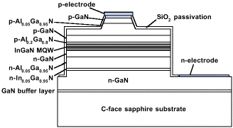
Another requirement for the p contact, as described earlier, is that it be transparent to light emission, which is accomplished by making it extremely thin to minimize absorption. AuNi films less than 0.03 µm thick are commonly used to obtain at least 50% light transmission at the wavelengths of interest. Metallizations suitable for commercial applications have additional requirements, such as superior adhesion to the semiconductor, good morphology, and excellent metallurgical reliability (low film stress, no intermetallic formation, corrosion resistance, thermal stability, etc.), which increase the challenge of finding a good system.
Ohmic contacts to n-type GaN are much easier to obtain than p-type ohmic contacts and do not have to be transparent. Many donors have low enough thermal-activation energies (22 meV for silicon)36 to be mostly ionized at room temperature, and it is easy to obtain high carrier concentrations. There are a number of publications on Schottky and ohmic contacts to n-type GaN.37 Most of the ohmic systems are based on aluminum or Ti/Al.38 Other interesting systems are indium-based,39 leading to InGaN formation after rapid thermal anneal through a solid-state reaction at the contact interface. The mechanism for ohmicity then relies on bandgap engineering arguments similar to the ones motivating the use of InGaAs layers on a GaAs surface to achieve barrierless current injection.40 The first reports of p-n junction blue LEDs produced from the III-nitride materials system came in 199141 with a homojunction GaN LED emitting blue light around 430 nm at an output power of 42µW at 20 mA. This blue light emission was from an impurity transition related to the magnesium-dopant in the p-GaN layer. The performance was several times higher than the best commercially available SiC blue LEDs at the time. The first GaN/InGaN/GaN double heterostructure LEDs, reported in early 1993,42 showed improved output power to 125µW at an emission wavelength of 440 nm, corresponding to the energy bandgap of the InGaN active region. Later reports in 199323 described devices with output power of more than 1,000µW and reduced operating voltage of approximately 3.6 V. The first commercial high-brightness candela-class blue LED products were released in late 1993 by Nichia Chemical Company and were described in the literature in early 1994.12 These commercial devices employed an intentional Zn-Si impurity complex in the InGaN active region to produce blue LEDs with a broad emission spectrum centered at 450 nm. The output power was as high as 1.5 mW, corresponding to an external quantum efficiency of 2.7% and a luminous efficiency of 2.1 lumens/watt. External quantum efficiency refers to the ratio of the number of photons produced to the electrical current crossing the pn-junction, in units of photons/electron. Luminous efficiency refers to the extent of the human-eye response per unit of input power to the LED. The human-eye response43 is greatest in the green spectral region and drops as the wavelength goes to the ultraviolet or infrared regions. By changing the epitaxial growth process slightly it was possible to produce LEDs with emission into the blue-green spectral region around 490 nm. However, there were two significant issues with these Zn-Si codoped LEDs. First, the emission wavelength blue-shifted with increasing operating current, leading to a noticeable shift in color. Second, the blue-green LEDs had a distinct whitish appearance due to the broad emission spectrum.
The current variety of high-brightness blue44 and green45 LEDs were reported during 1995. This second generation of commercial III-V nitride LED products, based on a SQW structure, dramatically improved the efficiency and the color purity for blue-green and green LEDs. Reported output power values for 450 nm blue and 525 nm green LEDs are 4.8mW and 3.0mW, respectively, corresponding to luminous-efficiency values of approximately 3.0 lumens/watt and 22.0 lumens/watt, respectively. Nichia Chemical Company of Japan has commercialized LEDs with this SQW structure and produces devices with wavelengths of 470 nm blue, 495 nm blue-green, and 525 nm green with efficiencies that significantly exceed these reported values.46 The spectral width of these commercial LEDs is significantly narrower than the first generation Zn-Si codoped LEDs and, hence, results in a greatly improved color purity or saturation. However, the shift of color with increasing operating current remains a concern for this technology. 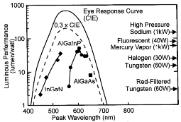
With the commercialization of InGaN quantum-well LEDs in the blue through green spectral regions, there now exists solid-state light sources spanning the entire visible spectral region. Figure 6 shows the luminous efficiency versus wavelength for the current state-of-the-art in commercially visible LEDs. High-brightness LEDs in the yellow-green through red-orange spectral region are commercially produced with the AlInGaP material system47 and in the red spectral region with the transparent-substrate AlGaAs material system.48 In addition, Figure 6 shows luminous-performance values for a number of conventional light sources and the human-eye response curve (CIE curve), which describes the theoretical limit for luminous efficiency. It is readily apparent that solid-state LEDs are rapidly encroaching upon the performance levels of traditional light sources and, in most cases, significantly exceed filtered filament-based light of a specific color. Several major markets are being addressed with these newly developed solid-state light sources. Automobile exterior lighting has been moving rapidly to incorporate transparent-substrate AlInGaP technology into high-mount stop lights and into the full amber and red-orange taillight assembly. Full-color, outdoor, changeable message signs and full-motion video displays have been adopting (AlIn)GaN and AlInGaP technologies and will continue to proliferate as costs are reduced. Traffic-signal applications have begun to incorporate red AlInGaP and AlGaAs LEDs for stop lights and are moving toward incorporating amber and blue-green LEDs to produce a completely LED-based signal head. All of these markets are rapidly expanding and will provide enormous growth opportunities in the future.
Fuente:
Nombre Franklin Quintero
Asignatura EES